 |
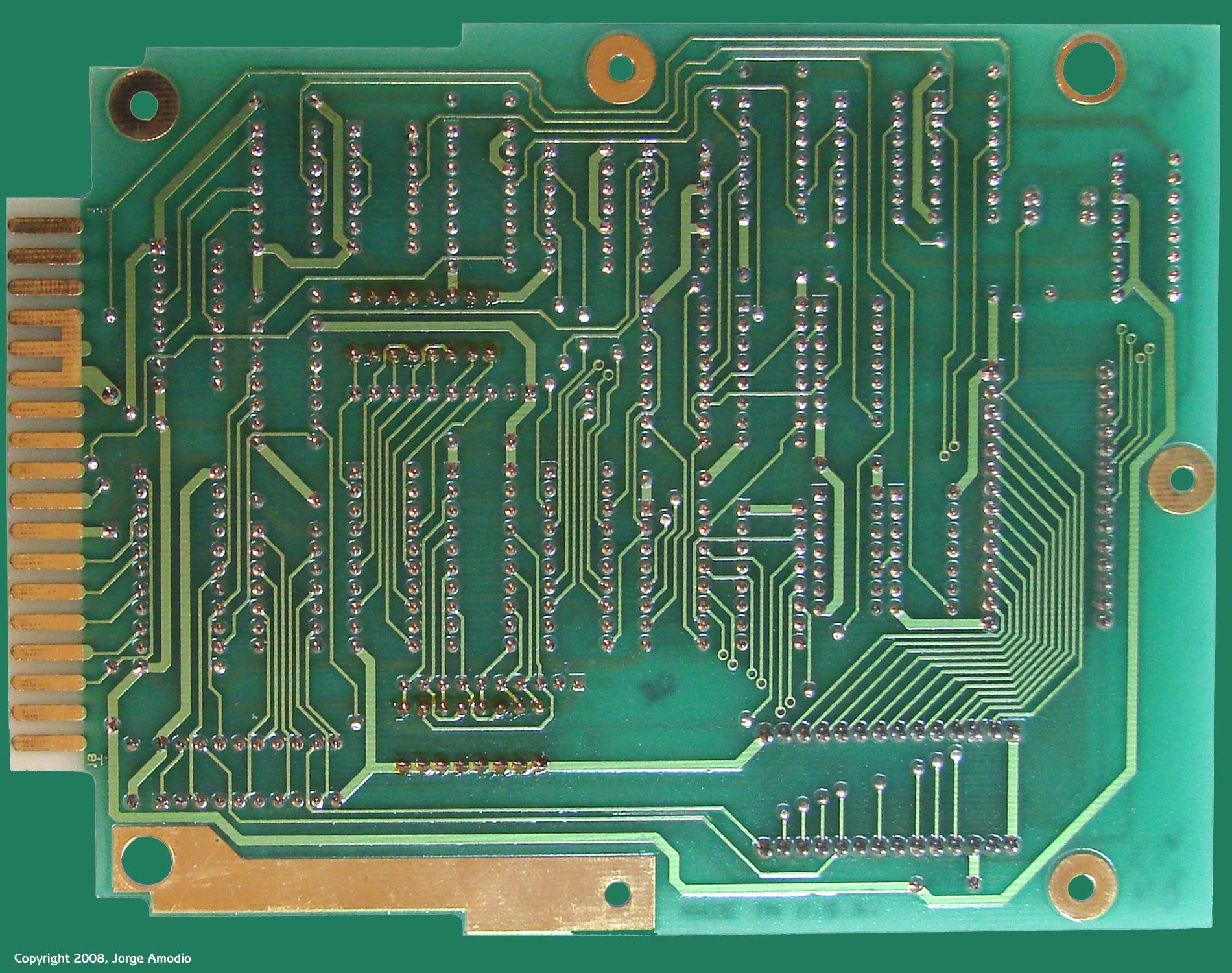
| HP 82929A Solder Side |
 |
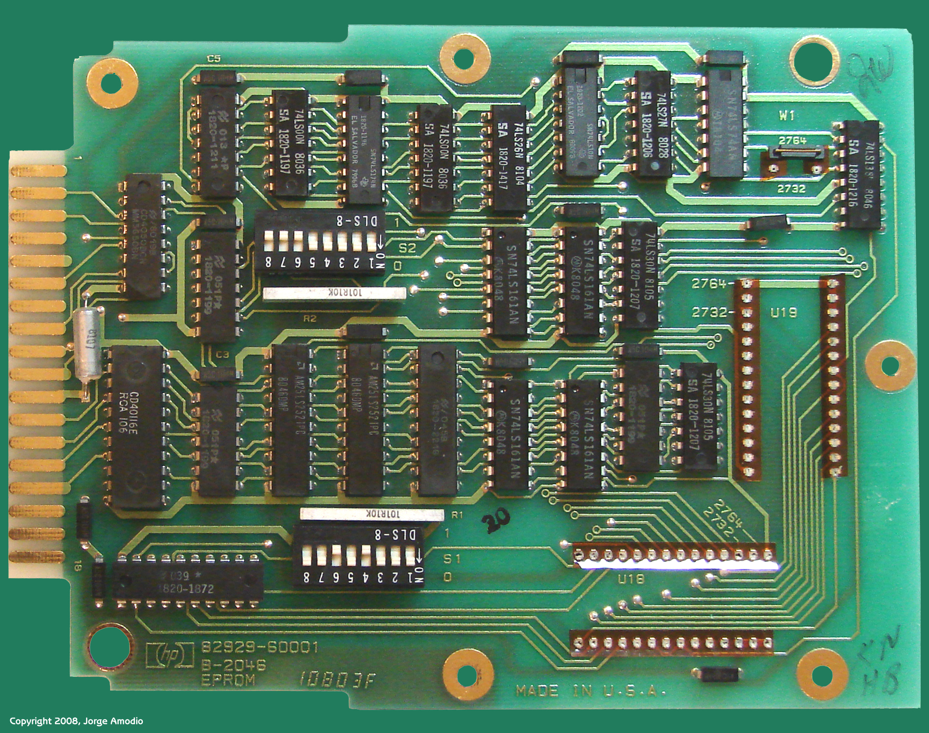
| HP8229A Component Side |
The module fits into one of the rear expansion slots and allows you to add your own code resident in PROM or EPROM, or any of the old original ROM modules for which images are available on-line.
After removing the enclosure of the HP 82929A module you will find two 28-pin DIP sockets that can accommodate either two 4KByte (2732) or two 8KByte (2764) EPROMs. Each ROM module image is 8KBytes, then using 2764 EPROMs you can add two additional ROM module images with the HP 82929A module.
Project Description
The primary goal of this project is to reverse engineer an original HP 29829A module and obtain a full set of schematics. Since the module does not require or use any specific custom HP parts only standard (some of the original ICs may be obsolete today and hard to find) CMOS and TTL parts it won't be hard having the schematics to make a clone or equivalent module.
Also having the schematics and a better understanding about how the HP-85 I/O bus works will provide valuable information for another project in the list that is to emulate many expansion modules and interfaces with a microcontroller based board.
This process has been done in the past, but besides some high level description of the PRM-85 developed by Bill Kotaska with support from John Shadbolt as a replacement for the HP 82929A, I didn't find much information available on-line.
John was quick to reply to my request for information, and I owe him a great deal of gratitude for his help and encouragement for this an other projects we discussed via e-mail. I also recently got in touch with Bill, we are already exchanging some information and ideas.
I also need to mention Everett Kaser who while at HP was involved somehow in the HP-85 development and provided additional information. When I was almost done with drawing the complete schematics Everett found and scanned the schematics for an old EPROM board that HP used to run the diagnostics code and for a 3 8-bit Digital Output ports. Both schematics helped to confirm and validate the one I was putting together.
Project Progress
I started putting together the schematics by following the traces using two high resolution pictures of the HP 82929A top and bottom sides posted by Vassilis Prevelakis in 2003 in the ClassicCMP mailing list.
Doing the solder or bottom side was obviously quite easy since you can see all the traces in front of your eyes, but getting the traces on the component or top side was a challenge. While the picture had good resolution some shadows on the ICs pins made it very difficult.
I was almost ready to hang the towel and keep searching for help on the net when John came to the rescue and let me put my hands on an actual and working HP 82929A module.
What I did first was to take high resolution pictures of both sides of the board. The pictures above on the right are a medium resolution version of the actual board. You can find a pair of higher resolution version in the links section below.
Now with the new pictures I sized them and mirrored the bottom side to match the top side. Using Adobe Pothoshop I created different layers for different elements such as pads and vias, top and bottom traces and legend for component IDs.
For the complicated and hidden traces on the component side I recurred to an ohm meter and also the logic that was showing up on the schematic I was putting together.
The following two pictures show the top and bottom sides and the pads, vias and trace layers for each side of the HP 82929A board.
 |
| Top side traces |
 |
| Bottom side traces |
 |
| HP 92829A PCB Layout |
Now with the complete board layout, time and patience was not too difficult to put the complete schematic together. It took me a couple of passes while I moved gates here and there to make the final schematic more easy to read and logically consistent.
As I do for many other projects I used Eagle CAD to enter the schematics and Adobe Acrobat to produce a pdf print out.
Project Status
As I do for many other projects I used Eagle CAD to enter the schematics and Adobe Acrobat to produce a pdf print out.
Project Status
This project is complete and the full schematics and additional information can be found in the links below.
Project Files and References
- HP 82929A Programmable ROM Drawer Schematics (by Jorge Amodio)
- HP 82929A Component Side High-Res Picture (1900x1500px ~2.4MB)
- HP 82929A Solder Side High-Res Picture (1900x1500px ~2.4MB)
- PRM-85 Module by Bill Kotaska and John Shadbolt
- HP EPROM Diagnostics Module Schematics (courtesy Everett Kaser)
- HP-85 Tripe 8-Bit Parallel Output Port Schematics (courtesy Everett Kaser)
- HP 82929A High Resolution Pictures by Vassilis Prevelakis
Thanks for your work on this! I put together a board using your design with a few modifications. I added 27512 support so I could use the PRM-85 SuperROM with 8 ROM images in one 27512. I designed a board using EagleCAD (Freemium version)and made a board with the toner-transfer method. I'm still working on it, but my initial test look like it should work fine. I'll report back with a link to my web site with this project when I get it on-line.
ReplyDeleteThanks for your comment Clay and glad to know that the information was useful for you. Feel free to send the link to your project I can add it to the main article.
ReplyDeleteFantastic work. Can you explain how this board compares to the PRM-85? Can you share the Eagle or Gerber files so one can reproduce it?
ReplyDeleteMarc
Oh I see from your other blog entry, you never made a PCB of it, just a wire wrap version? Are the Eagle CAD schematc files available anywhere in native fornat (not pdf)?
ReplyDeleteJorge,
ReplyDeletethank you for the work! Did you ever publish the EAGLE files so that one could reproduce the board? Any plans to make them available or other files suitable for manufacturing the PCB?
This could be a simple do-it-yourself alternative to the more elaborate PRM-85 board, which is great but also rather complex.
Martin
Thanks for doing this. Do you have any information on the bus timing? I'm thinking of building a PIC-based ROM emulator.
ReplyDeleteThanks
Brian
Thanks for the schmatics, note the PRM-85 webpage has moved, curently on vintagecomuters.site90.net
ReplyDeleteThank y'all for your comments, I've not been paying much attention to the Blog in the past few years but I'm slowly getting back into some projects and the habit of writing about them. Very often time is a limited resource to be able to complete as much as I'd wish.
ReplyDeleteI updated the link to the PRM-85 page and I'll try to answer some of your questions soon. I've not done much more with my collection of HP-80's and I still have in mind putting something together with a high performance MCU or FPGA. I've seen some interesting ideas circulating on various related mailing lists. Thanks again and stay tuned !!